Comparative studies for determining the optical band gap energy of CuSe thin films

Authors

  • O. O. Olasanmi Department of Physics, Faculty of Physical Sciences, University of Ilorin, Ilorin, Kwara State, Nigeria
  • S. I. Akinsola Department of Physics, Faculty of Physical Sciences, University of Ilorin, Ilorin, Kwara State, Nigeria
  • K. A. Yusuf Department of Physics, Faculty of Physical Sciences, University of Ilorin, Ilorin, Kwara State, Nigeria
  • A. E. Aregbesola Department of Mathematics, Statistics, and Physics, Wichita State University, 1845 Fairmount St. Wichita, KS 67260, United States of America

Keywords:

Selenium, Tauc’s relation, Band gap, Structural property, Thermal evaporation

Abstract

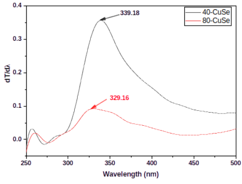
In the present study, copper selenide (CuSe) metal chalcogenide thin films have been fabricated from Se/Cu bilayer deposited using two-step procedure involving thermal evaporation and dip coating followed by thermal annealing. The thermally evaporated Se layer was maintained at a constant thickness of 40 nm while the dip coated layer of copper was carried out for varying time of 40 and 80 min. The prepared CuSe thin film was characterized in terms of its structural and optical properties. The X-ray diffraction spectra revealed post thermal inter-diffusion of the two layers and the production of CuSe thin film exhibiting hexagonal crystal structure. The optical transmission measurements were recorded within the wavelength range of 300 to 1000 nm. Four different methods were employed in ascertaining the direct band gap energies of the prepared CuSe thin films and the results were compared with the famous Tauc’s relation. The values of the band gap energy ranges between 3.58 and 3.87 eV for the 40-CuSe sample as well as 3.65 and 3.99 eV for the 80-CuSe sample. The results from the study confirmed that the fabricated films possess wide band gap energy, making them a candidate for window layer in many solar cell applications.

Dimensions

[1] A. Talaat, S. H. Hameed, H. Moustafa, B. A. Shaban, A. Mansour & B. A. Hameed, ‘‘The effect of selenium on the structural, morphology, optical, electrical properties of Cu2 Te thin films for thermoelectric and photovoltaic applications’’, Optical Materials 109 (2020) 110308. https://doi.org/10.1016/j.optmat.2020.110308.

[2] S. R Gosavi, N. G. Deshpande, Y. G. Gudagea & R. Sharma, ‘‘Physical, optical and electrical properties of copper selenide (CuSe) thin films deposited by solution growth technique at room temperature’’, Journal of Alloy and Compound 448 (2008) 344. http://dx.doi.org/10.1016/j.jallcom.2007.03.068.

[3] F. Yakuphanoglu & C. Viswanathan, ‘‘Electrical conductivity and single oscillator model properties of amorphous CuSe semiconductor thin film’’, Journal of Non-Crystal Solids 353 (2007) 2934. https://doi.org/10.1016/j.jnoncrysol.2007.06.055.

[4] C. L. J. Ying, Z. A. Talib, W. Mahmood, M. Yunus, Z. Zainal, S. A. Halim, M. M. Moksin, W. M. Yussof & K. P. Lim, ‘‘Structural, morphology and electrical properties of layered copper selenide thin film’’, Central European Journal of Physics. 7 (2009) 379. https://doi.org/10.2478/s11534-009-0057-1.

[5] V. Y. Kogai & G. M. Mikheev, ‘‘Controlled synthesis of a textured CuSe (006) film by vacuum thermal treatment of a Se/Cu film structure’’, Technical Physics Letters 49 (2023) 25. http://dx.doi.org/10.61011/TPL.2023.06.56373.19451.

[6] H. K, Sadekar, ‘‘Optical and structural properties of CuSe thin films deposited by chemical bath deposition (CBD) technique’’, International Research Journal of Science & Engineering, Special Issue A2 (2018) 20, http://www.irjse.in/.

[7] S. Kim, Y. S. Lee & N. H. Kim, ‘‘Homogeneity- and stoichiometry-induced electrical and optical properties of Cu-Se thin films by RF sputtering power’’, Materials 16 (2023) 6087. https://doi.org/10.3390/ma16186087.

[8] R. S. Meshram, ‘‘Structural and morphological properties of CuSe thin films prepared by spray pyrolysis technique’’, Journal of emerging technology innovation and Research 8 (2021) 445. https://www.jetir.org/papers/JETIR2112153.pdf.

[9] Y. Hu, M. Afzaal, M. A. Malik & P. O’Brien, ‘‘Deposition of copper selenide thin films and nanoparticles’’, Journal of Crystal Growth 297 (2006) 61. http://dx.doi.org/10.1016/j.jcrysgro.2006.08.038.

[10] R. A. Hussain & I. Hussain, ‘‘Copper selenide thin films from growth to applications’’, Solid State Science 100 (2020) 106101. https://doi.org/10.1016/j.solidstatesciences.2019.106101.

[11] D. Souri, A. R. Khezripour, M. Molaei & M. Karimipour, ‘‘ZnSe and copper-doped ZnSe nanocrystals (NCs): optical absorbance and precise determination of energy band gap beside their exact optical transition type and Urbach energy’’, Current Applied Physics 17 (2016) 41. https://doi.org/10.1016/j.cap.2016.10.008.

[12] D. Souri & V. Tahan, ‘‘A new method for the determination of optical band gap and the nature of optical transitions in semiconductors’’, Applied Physics B 119 (2015) 273. https://doi.org/10.1007/s00340-015-6053-9.

[13] B. A. Bader, S. K. Muhammad, A. M. Jabbar, K. H. Abass, S. S. Chiad & N. F. H. Bader, ‘‘Synthesis and characterization of indium-doped CdO nanostructured thin films: a study on optical, morphological, and structural properties’’, Journal of Nanostructure 10 (2020) 744. http://dx.doi.org/10.22052/JNS.2020.04.007.

[14] A. McInnes, J. S. Sagu & D. Mehta, ‘‘Low-cost fabrication of tunable band gap composite indium and gallium nitrides’’, Scientific Report 9 (2019) 2313. https://doi.org/10.1038/s41598-019-38882-3.

[15] D. Rajesh, R. R. Chandrakanth & C. S. Sunandana, ‘‘Annealing effects on the properties of copper selenide thin films for thermoelectric applications’’, IOSR journal of applied Physics 4 (2013) 65. http://dx.doi.org/10.9790/4861-0456571.

[16] A. M. El Nahrawy, A. M. Mansour, A. B. A. Hammad & A. R. Wassel, ‘‘Effect of Cu incorporation on morphology and optical band gap properties of nano-porous lithium magneso-silicate (LMS) thin films’’, Material Research Express 6 (2018) 016404 https://doi.org/10.1088/2053-1591/aae343.

[17] R. Raciti, R., Bahariqushchi, C. Summonte, A. Aydinli, A. Terrasi & S. Mirabella, ‘‘Optical bandgap of semiconductor nanostructures: methods for experimental data analysis’’, Journal of Applied Physics 121 (2017) 234304. https://doi.org/10.1063/1.4986436.

[18] L. E. Alarcon, A. Arrieta, E. Camps, S. Muhl, S. Rudil & E. V. Santiago, ‘‘An alternative procedure for the determination of the optical band gap and thickness of amorphous carbon nitride thin films’’, Applied Surface Science 254 (2007) 412. https://doi.org/10.1016/j.apsusc.2007.07.052.

[19] D. M. Mamand, D. S. Muhammad, D. Q. Muheddin, K. A. Abdalkarim, D. A. Tahir, H. A. Muhammad, S. B. Aziz, S. A. Hussen & J. Hassan, ‘‘Optical band gap modulation in functionalized chitosan biopolymer hybrids using absorption and derivative spectrum fitting methods’’, A spectroscopic analysis, Scientific Reports 15 (2025) 3162. https://doi.org/10.1038/s41598-025-87353-5.

[20] S. H. Elazoumi, H. A. A. Sidek, Y. S. Rammah, R. El-Mallawany, M. K. Halimah, K. A. Matori & M. H. M. Zaid, ‘‘Effect of PbO on optical properties of tellurite glass’’, Results in Physics 8 (2018) 16. https://doi.org/10.1016/j.rinp.2017.11.010.

[21] S. Ilican ‘‘Improvement of the crystallinity and optical parameters of ZnO Film with aluminum doping’’, Anadolu University Journal of Science and Technology A-Applied Sciences and Engineering 17 (2016) 181. https://doi.org/10.18038/btda.45168.

[22] K. Ramesh, S. Thanikaikarasan & B. Bharathi, ‘‘Structural, morphological and optical properties of copper selenide thin films’’, International Journal of Chemtech Research 6 (2014) 5408. https://www.researchgate.net/publication/287302365_Structural_morphological_and_optical_properties_of_copper_selenide_thin_films.

Published

2025-03-19

How to Cite

Comparative studies for determining the optical band gap energy of CuSe thin films. (2025). Proceedings of the Nigerian Society of Physical Sciences, 2(1), 191. https://doi.org/10.61298/pnspsc.2025.2.191

How to Cite

Comparative studies for determining the optical band gap energy of CuSe thin films. (2025). Proceedings of the Nigerian Society of Physical Sciences, 2(1), 191. https://doi.org/10.61298/pnspsc.2025.2.191